Asus NVIDIA Geforce 7950 GX2 - GPU G71
Last Update: March 3, 2007
� Back To GPU Database
[ Index ]Introduction | 2 | 3 | 4 | 5 | 6 | 7 | 8 | 9 | 10 | 11 | 12 | 13 | 14 | 15
�Next Page
5 - 7950 GX2: Features / GPU Info

| GPU | G71 |
| Designation | EN7950GX2212PHT/1G/A |
| Transistors Count | 278 million |
| Manufacturing Process | 90 nm |
| GPU Frequency | 500 MHz |
| Memory Frequency | 600 MHz |
| Memory Type | GDDR3 |
| Memory Interface | 256 bits |
| Memory Size | 1024Mb |
| Shader Model Version | 3.0 |
| OpenGL Version | 2.0 |
| Direct3D Version | 9.0 |
| Vertex Pipelines | 2x8 |
| Pixel Pipelines | 2x24 |
| ROPs | 2x16 |
| Texture Units | 16 |
| Texture Max Size | 4096x4096 |
| FSAA | 2X / 4X / 6X / 8X / 16X |
| Slot | PCI-Express |
RivaTuner Report:
$ffffffffff ----------------------------------------------------------------
$ffffffffff Display adapter information
$ffffffffff ----------------------------------------------------------------
$0000000000 Description : NVIDIA GeForce 7950 GX2
$0000000001 Vendor ID : 10de (NVIDIA)
$0000000002 Device ID : 0294
$0000000003 Location : bus 9, device 0, function 0
$0000000004 Bus type : PCIE
$000000000f PCIE link width : 16x supported, 8x selected
$0000000009 Base address 0 : fb000000 (memory range)
$000000000a Base address 1 : c0000000 (memory range)
$000000000b Base address 2 : none
$000000000c Base address 3 : fa000000 (memory range)
$000000000d Base address 4 : none
$000000000e Base address 5 : 0000dc00 (I/O range)
$ffffffffff ----------------------------------------------------------------
$ffffffffff NVIDIA specific display adapter information
$ffffffffff ----------------------------------------------------------------
$0100000000 Graphics core : NV49/G71 revision A2 (24pp,8vp)
$0100000001 Hardwired ID : 0290 (ROM strapped to 0294)
$0100000002 Memory bus : 256-bit
$0100000003 Memory type : DDR3 (RAM configuration 03)
$0100000004 Memory amount : 524288KB
$0100000100 Core clock domain 0 : 499.500MHz
$0100000101 Core clock domain 1 : 499.500MHz
$0100000102 Core clock domain 2 : 499.500MHz
$0100000006 Memory clock : 600.750MHz (1201.500MHz effective)
$0100000007 Reference clock : 27.000MHz
$ffffffffff ----------------------------------------------------------------
$ffffffffff NVIDIA VGA BIOS information
$ffffffffff ----------------------------------------------------------------
$1100000000 Title : ASUS EN7950GX2 VGA
BIOS Version 5.71.22.24.AS01
$1100000002 Version : 5.71.22.24.05
$1100000100 BIT version : 1.00
$1100000200 Core clock : 500MHz
$1100000201 Memory clock : 600MHz
$1100010000 Performance level 0 : 500MHz/600MHz/1.25V/40%
$1100020000 VID bitmask : 00000111b
$1100020100 Voltage level 0 : 1.25V, VID 00000000b
$1100030001 Core thermal compensation : 8�C
$1100030002 Core thermal threshold : 122�C
$1100030004 Thermal diode gain : 0.046�C
$1100030005 Thermal diode offset : -250.510�C
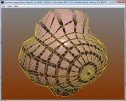
GPU Caps Viewer:

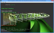
ATITool:
- Core Clock: 500MHz
- Memory Clock: 600MHz

RivaTuner:
- Core Clock: 499.50MHz
- Memory Clock: 600.75MHz
 [ Index ]
Introduction | 2 | 3 | 4 | 5 | 6 | 7 | 8 | 9 | 10 | 11 | 12 | 13 | 14 | 15
�Next Page